- 您现在的位置:买卖IC网 > Sheet目录505 > RXM-GPS-SR-T (Linx Technologies Inc)GPS MODULE SMD SIRF W/ANT
�� �
�
�BOARD� LAYOUT� GUIDELINES�
�The� module’s� design� makes� integration� straightforward;� however,� it� is� still� critical�
�to� exercise� care� in� PCB� layout.� Failure� to� observe� good� layout� techniques� can�
�result� in� degradation� of� the� module’s� performance.� Grounding,� filtering,�
�decoupling,� routing� and� layer� order� are� important� considerations� for� any� RF�
�design.� The� following� section� provides� some� basic� design� guidelines� which� may�
�be� helpful.�
�During� prototyping,� the� module� should� be� soldered� to� a� properly� laid-out� circuit�
�board.� The� use� of� prototyping� or� “perf”� boards� will� result� in� poor� performance� and�
�is� strongly� discouraged.�
�The� module� should,� as� much� as� reasonably� possible,� be� isolated� from� other�
�components� on� your� PCB,� especially� high-frequency� circuitry� such� as� crystal�
�oscillators,� switching� power� supplies,� and� high-speed� bus� lines.�
�When� possible,� separate� RF� and� digital� circuits� into� different� PCB� regions.� Make�
�sure� internal� wiring� is� routed� away� from� the� module� and� antenna,� and� is� secured�
�to� prevent� displacement.�
�Do� not� route� PCB� traces� directly� under� the� module.� There� should� not� be� any�
�copper� or� traces� under� the� module� on� the� same� layer� as� the� module,� just� bare�
�PCB.� The� underside� of� the� module� has� traces� and� vias� that� could� short� or� couple�
�to� traces� on� the� product’s� circuit� board.�
�The� Pad� Layout� section� shows� a� typical� PCB� footprint� for� the� module.� A� ground�
�plane� (as� large� and� uninterrupted� as� possible)� should� be� placed� on� a� lower� layer�
�of� your� PC� board� opposite� the� module.�
�Vias� are� acceptable� for� tying� together� ground� layers� and� should� be� used� in�
�multiples.�
�Each� of� the� module’s� ground� pins� should� have� short� traces� tying� immediately� to�
�the� ground� plane� through� a� via.�
�ANTENNA� CONSIDERATIONS�
�The� SR� Series� module� has� an� integral� ceramic� patch� antenna.� This� eliminates�
�the� need� for� any� external� RF� components� and,� in� some� respects,� simplifies� the�
�design� process.� While� convenient,� an� on-board� antenna� makes� factors� such� as�
�layout,� placement� and� product� packaging� much� more� critical.� The� antenna’s�
�performance� plays� a� major� role� in� determining� realized� sensitivity.� In� order� for� the�
�module� to� perform� correctly� it� is� essential� that� the� antenna� be� given� proper�
�consideration.� Due� to� the� compact� size� of� the� antenna,� it� may� be� necessary� for�
�the� antenna� to� be� tuned� specifically� in� the� end� product� environment.� If� this� is� the�
�case,� Linx� can� assist� with� layout� and� obtaining� a� custom� tuned� antenna.�
�Following� these� guidelines� will� help� to� achieve� the� best� antenna� performance.�
�The� antenna� element� should� be� inside� the� product� or� covered� to� prevent� damage�
�to� it.� The� center� frequency� of� the� antenna� will� be� affected� by� materials� in� close�
�proximity� to� it.� The� product’s� housing� should� not� come� within� approximately� 0.25”�
�of� any� antenna� surface.� The� housing� must� also� be� RF� transparent,� i.e.� non-�
�metallic,� no� metal� paint,� fillers� or� compositions� which� would� impede� RF� at� the�
�frequencies� of� interest.� The� antenna� should� never� be� encapsulated,� coated,� or�
�sprayed� with� any� compound.�
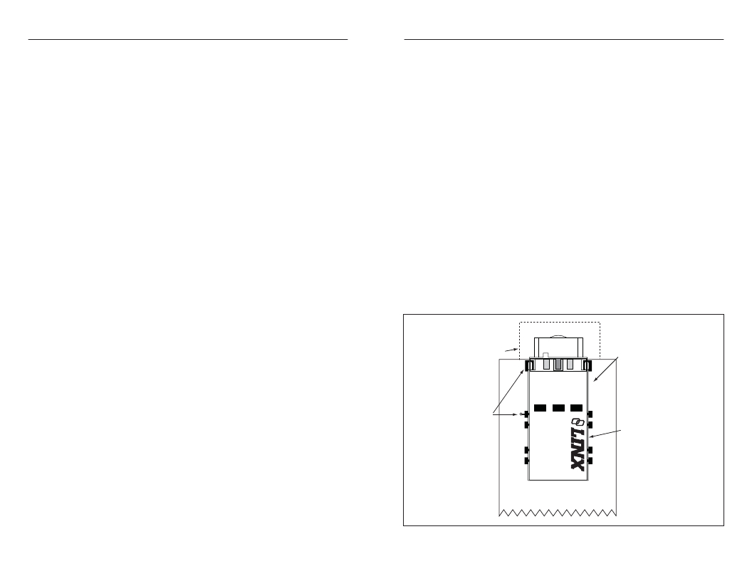
�Ideally,� the� antenna� will� sit� at� the� edge� of� the� PCB� and� have� no� other�
�components� to� the� top� or� sides� as� illustrated� below.� If� it� is� necessary� to� place�
�components� adjacent� to� the� antenna,� try� to� maintain� a� 0.25”� or� greater� setback�
�and� recognize� performance� may� be� adversely� affected.� It� is� a� good� idea� to� test�
�your� design’s� performance� against� a� benchmark.� This� will� help� to� identify� any�
�performance� issues� and� the� impact� of� design� tradeoffs.� A� GPS� module� placed�
�on� an� optimized� PCB� with� no� external� housing,� or� the� Linx� MDEV� GPS�
�evaluation� system,� can� be� used� as� a� helpful� point� of� reference.�
�Bypass� caps� should� be� low� ESR� ceramic� types� and� located� directly� adjacent� to�
�the� pin� they� are� serving.�
�The� integral� antenna� is� susceptible� to� external� influences.� Please� carefully� read�
�and� follow� the� guidelines� listed� in� the� section� titled� Antenna� Considerations.�
�In� some� instances,� a� designer� may� wish� to� encapsulate� or� “pot”� the� product.�
�There� is� a� wide� variety� of� potting� compounds� with� varying� dielectric� properties.�
�Since� such� compounds� can� considerably� impact� RF� performance� and� the� ability�
�to� rework� or� service� the� product,� it� is� the� responsibility� of� the� designer� to� evaluate�
�and� qualify� the� impact� and� suitability� of� such� materials.� UNDER� NO� CONDITION�
�SHOULD� THE� ANTENNA� ELEMENT� BE� POTTED� OR� ENCAPSULATED� IN�
�ANY� MANNER.�
�Page� 22�
�0.25� ”� minim� u� m� cle� a� r� a� nce�
�on� the� top� a� nd� s� ide� s�
�Tie� gro� u� nd� pin� s�
�individ� ua� lly� to� the�
�gro� u� nd� pl� a� ne�
�Loc� a� te� the� mod� u� le�
�a� w� a� y� from� noi� s� e�
�gener� a� ting� or� b� e� a� ring�
�component� s� or� tr� a� ce� s�
�Figure� 6:� Antenna� Considerations�
�Prod� u� ct� PCB�
�Avoid placing components�
�to� the� s� ide� s� of� the� mod� u� le�
�No� tr� a� ce� s� or� copper�
�u� nder� the� mod� u� le� on� the�
�sa� me� l� a� yer� as� the� mod� u� le�
�Page� 2� 3�
�发布紧急采购,3分钟左右您将得到回复。
相关PDF资料
RZE002P02TL
MOSFET P-CH 20V 200MA EMT3
RZF020P01TL
MOSFET P-CH 12V 2A TUMT3
RZF030P01TL
MOSFET P-CH 12V 3A TUMT3
RZM002P02T2L
MOSFET P-CH 20V 0.2A UMT6
RZQ045P01TR
MOSFET P-CH 12V 4.5A TSMT6
RZQ050P01TR
MOSFET P-CH 12V 5A TSMT6
RZR020P01TL
MOSFET P-CH 12V 2A TSMT3
RZR040P01TL
MOSFET P-CH 12V 4A TSMT3
相关代理商/技术参数
RXM-UHF
制造商:RADIOMETRIX 制造商全称:RADIOMETRIX 功能描述:UHF Radio Telemetry Receiver Module
RXP0005
制造商:Panasonic Industrial Company 功能描述:ARM
RXP0014
制造商:Panasonic Industrial Company 功能描述:PULLEY
RXP0015
制造商:Panasonic Industrial Company 功能描述:ROLLER
RXP0016
制造商:Panasonic Industrial Company 功能描述:ROLLER
RXP0016-4
制造商:Panasonic Industrial Company 功能描述:ROLLER
RXP0017
制造商:Panasonic Industrial Company 功能描述:ROLLER
RXP0017-3
制造商:Panasonic Industrial Company 功能描述:ROLLER